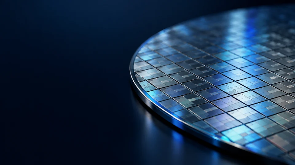
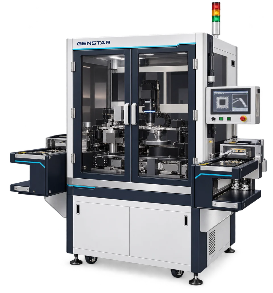
We combine optical inspection, X-ray imaging and vision AI for precision inspection. Industrial language models make manufacturing data easier to query, analyze and apply.
Support quality and efficiency in manufacturing through precision inspection, industrial vision and intelligent sensing, and industrial LLM applications.
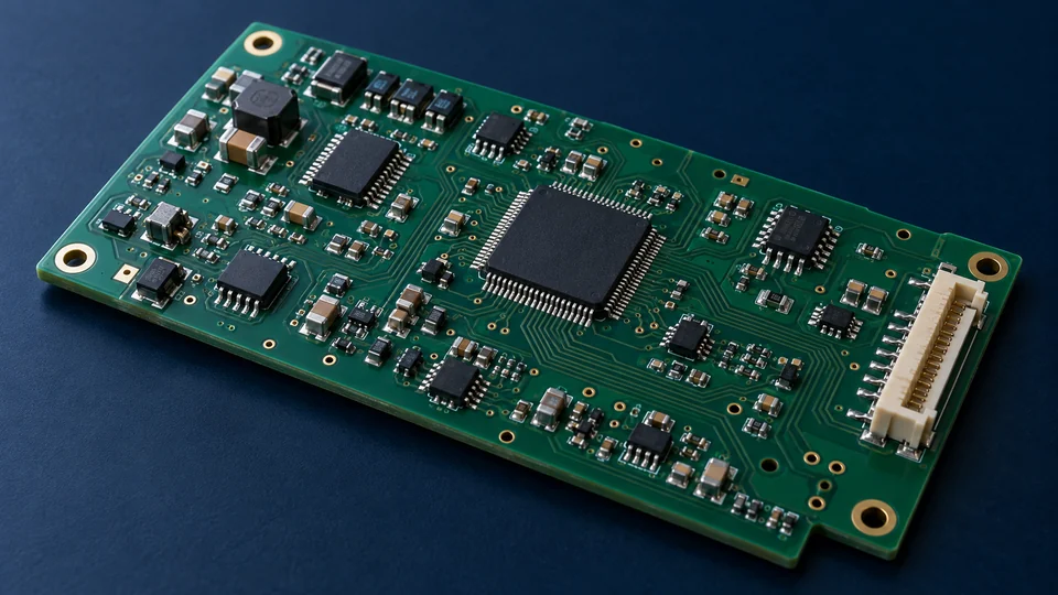
Inspect component appearance, assembly position and solder quality on PCBs and electronic assemblies. Observe internal structures to support analysis and review of complex defects.
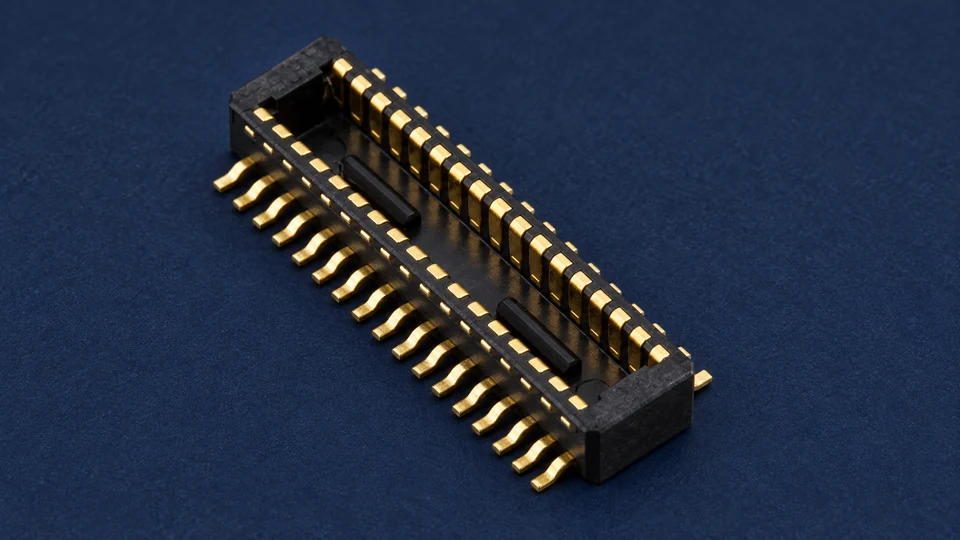
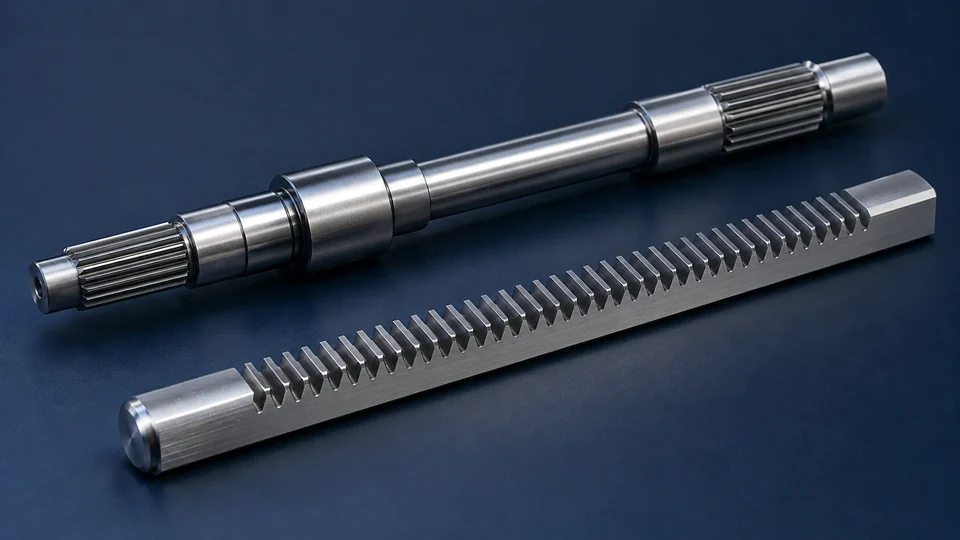
Inspect surface defects, foreign material, contacts and geometric profiles in electronic connectors and other precision components, focusing on quality differences in fine structures.
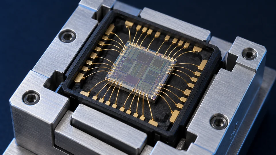
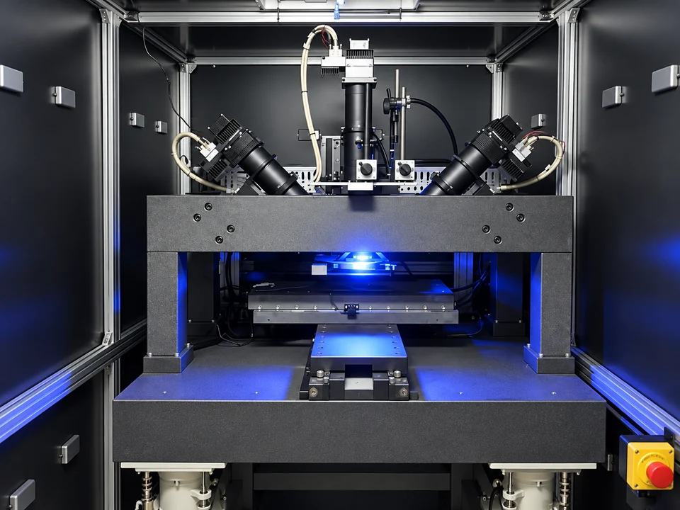
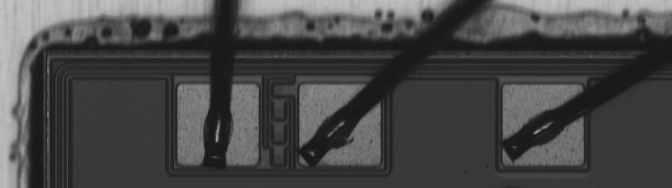
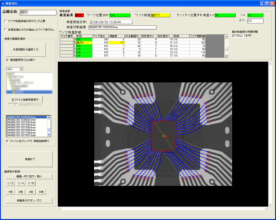
Combine 2D visual inspection and 3D geometry measurement for semiconductor wires and bonds. Inspect wire bends, shorts and breaks, as well as bond position, shape and foreign material.
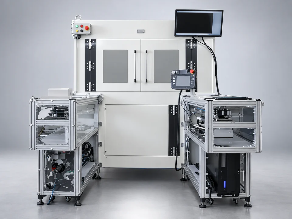
Inspect wires and bond regions concealed by molding with X-ray projections. Build checks around wire shape, continuity and neighboring wires, with feeding, handling and sorting configured for the workpiece.
Classify bond shapes from inspection images with vision AI, using contour and shape features to support appearance assessment.
WireBond · 2D metrology
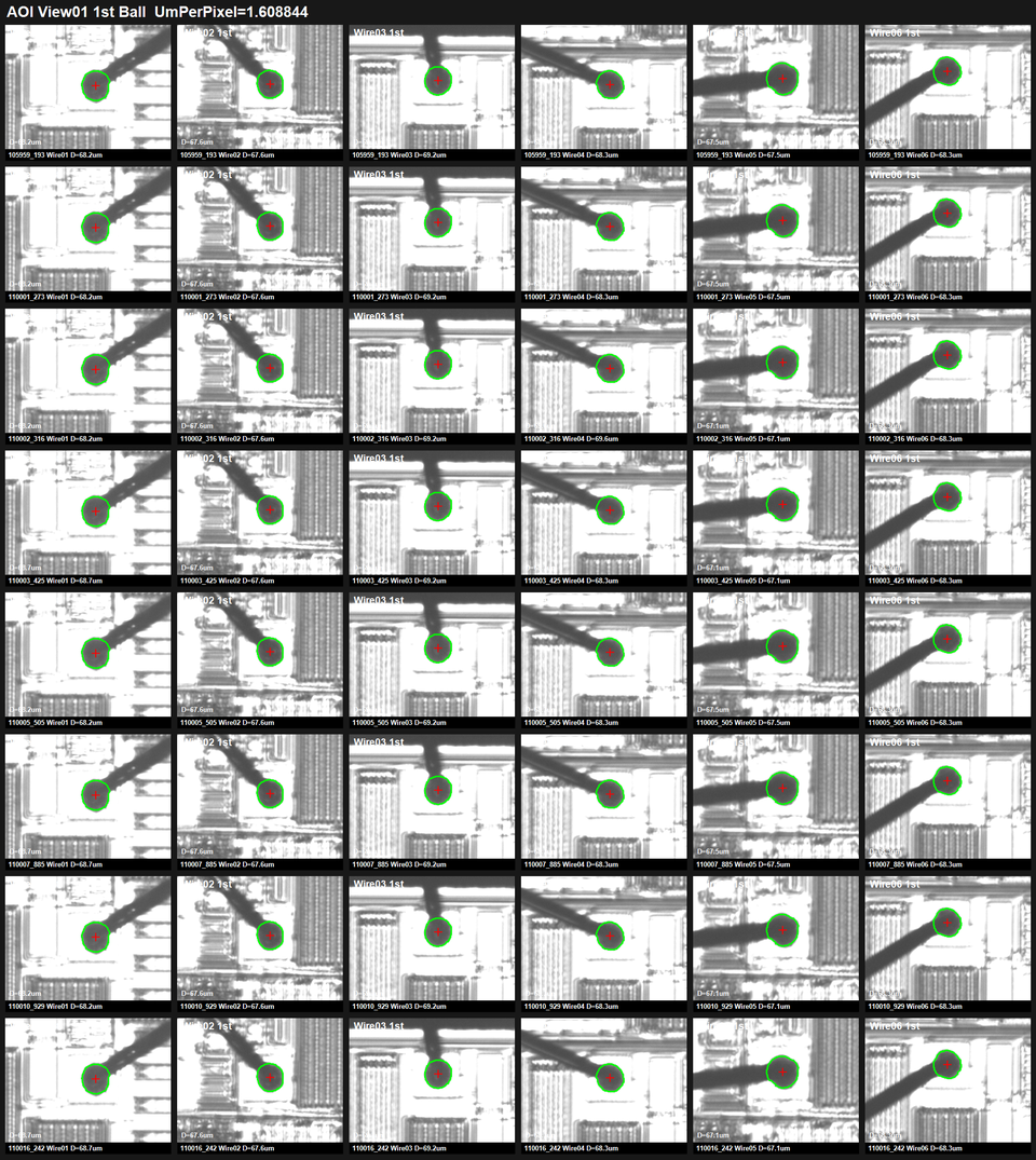
Bond geometry measurement
Locate bond centers and measure ball diameter and bond width. Compare repeated acquisitions to examine measurement consistency.
WireBond · Optical 3D
3D wire trajectory & loop height
Reconstruct wire trajectories from images at different focal planes and extract relative loop height to reveal the wire geometry in space.
MicroBump · Morphology
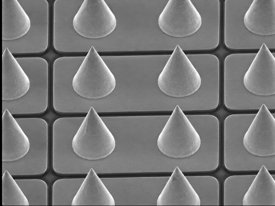
Pointed microbump morphology
Examine tip contours, array arrangement and local shapes to compare bump morphology and identify the structures for 3D measurement.
MicroBump · 3D metrology
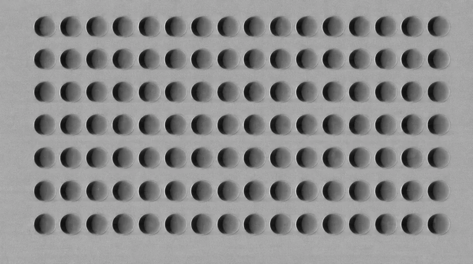
Microbump diameter & height
Measure microbump diameter, height and 3D shape with multiple projections and shadow-profile metrology to assess array geometry consistency.
WireBond · X-ray inspection
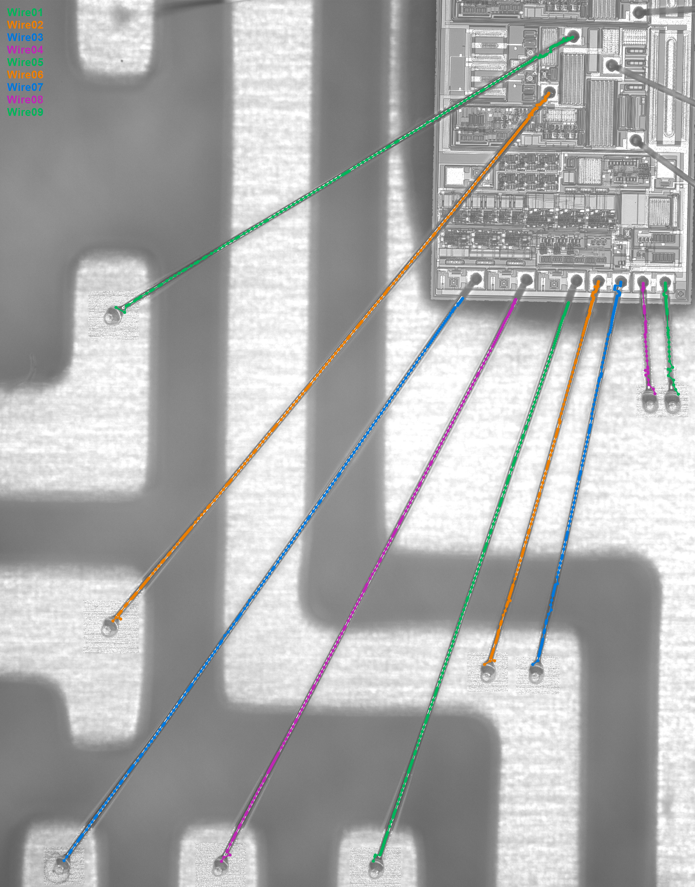
Internal package wire inspection
Use X-ray imaging and image processing to trace wire paths, inspect wire shape and arrangement, and observe structures inside semiconductor packages.
ABOUT GENSTAR
Precision inspection. Connected to manufacturing.
GENSTARINSPECTION & INTELLIGENCE
We actively expand into overseas markets and serve Japanese manufacturers.
GENSTAR brings together optical design, inspection equipment, AI algorithms and quality analytics. We focus on semiconductors and advanced packaging, with applications in precision manufacturing and automotive components. Teams in Hangzhou, Tianjin, Hamamatsu, Tokyo and Kyoto collaborate on development and engineering, from sample evaluation to system integration.